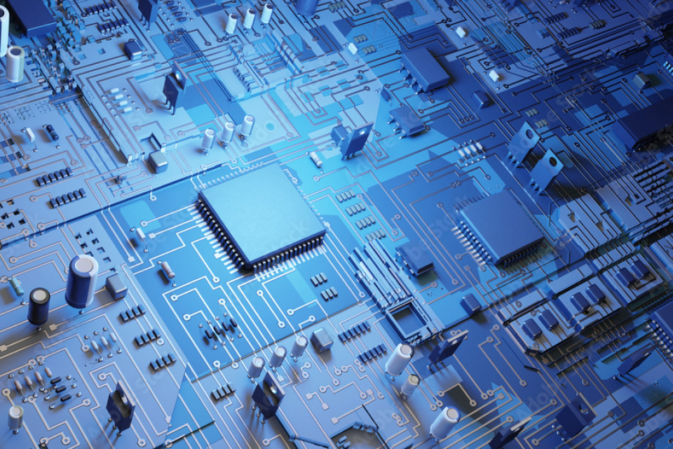
Facing the challenges of miniaturization and high integration with flattening technologies
Too small for the human eye. Advanced flattening technology used in the nanometer world

Circuits in semiconductors are wired in multiple layers and cannot be stacked accurately if they have even slight roughness. As a result, a process is used to repeatedly flatten the surface. CMP systems, one of the EBARA Group's semiconductor manufacturing systems, aid the flattening process and boast the second-largest global market share.

CMP systems perform a series of steps to flatten the wafer and clean and dry it. Because the wiring width is measured in nanometers (nm), flattening accuracy is also required in nanometers. Specifically, for a wafer with a diameter of 30 cm, the required flattening accuracy is within 10 nm, which is equivalent to the irregularity of 5 mm on the inner side of the Yamanote rail line (with an average diameter of 10 km). This high-precision flattening technology contributes to the high integration of state-of-the-art semiconductor devices.
These technologies produced by the Precision Machinery Company have been realized through continuous development in close cooperation with our customers since the first CMP system was shipped in 1992. The EBARA Group will continue to devote itself to technology development for cutting-edge semiconductor manufacturing.
These technologies produced by the Precision Machinery Company have been realized through continuous development in close cooperation with our customers since the first CMP system was shipped in 1992. The EBARA Group will continue to devote itself to technology development for cutting-edge semiconductor manufacturing.